PAM Review: Energy Science & Technology, Vol. 5
ISSN 2205-5231 | Published by UTS ePRESS | https://epress.lib.uts.edu.au/student-journals/index.php/PAMR/index
Analysis of Thermodynamic Properties of Cu(In,Ga)Se2 Thin-Film Solar Cells for Viable Space Application
Declan Clarke1 and Rodrigo Breguel2*
University of Technology Sydney, Faculty of Science, PO Box 123, Ultimo NSW 2017, Australia
1 declan.clarke@student.uts.edu.au
2 rodrigoignacio.breguelgallaher@student.uts.edu.au
Corresponding author: Rodrigo Breguel, University of Technology Sydney, Faculty of Science, PO Box 123, Ultimo NSW 2017, Australia; rodrigoignacio.breguelgallaher@student.uts.edu.au
DOI: http://dx.doi.org/10.5130/pamr.v5i0.1501
Citation: Clarke, D. and Breguel, R. 2018. Analysis of Thermodynamic Properties of Cu(In,Ga)Se2 Thin-Film Solar Cells for Viable Space Application. PAM Review: Energy Science & Technology, Vol. 5, pp. 131-149. http://dx.doi.org/10.5130/pamr.v5i0.1501
© 2018 by the author(s). This is an Open Access article distributed under the terms of the Creative Commons Attribution 4.0 International (CC BY 4.0) License (https://creativecommons.org/licenses/by/4.0/), allowing third parties to copy and redistribute the material in any medium or format and to remix, transform, and build upon the material for any purpose, even commercially, provided the original work is properly cited and states its license.
Abstract
The use of thin film solar cells for power generation when colonizing space stations is an interesting idea. Resisting harsh space environments and low power to mass ratio shows potential for the future application of thin film solar cell in future space application such as roll able solar blankets. Cu(In,Ga)Se2 thin film solar cell are analyzed to determine their viability in space focusing on two modular aspects of emissivity and buffer lays. Findings and calculations showed how temperature affects the efficiency of solar cells and it could also be found how increasing their emissivity with different kinds of coatings can offset the loss in efficiency. Through the study of buffers, it was found that lower band gaps reduce the quantum efficiency of a solar cell. Therefore, ZnS with an energy band gap of 3.5eV will have the least amount of spectral absorption of higher wavelengths.
Keywords
Cu(In,Ga)Se2; CdS; buffers; emissivity; efficiency; temperature
Introduction
In this meta study we will be identifying factors that have to be focused on before a cell can be viable for space application. The one such issue it thermal cycles and loads on solar cells in space. Reducing internal temperatures of solar cells will increase the efficiency, on way of reducing temperatures is emissivity. The study shows how the emissivity reduces the thermal loads on thermal cells in 𝐶𝑢(𝐼𝑛, 𝐺𝑎)𝑆𝑒, cells. The electrical performance of a (𝐼𝑛, 𝐺𝑎), cells have to compete with other flexible cells to be used in space, therefore the effect of recombination and buffer layers are studied showing high currents and ideal electrical properties are factors of buffer layers.
Solar Powered Satellites For Space Residence
On the Dec 18th 2018 International Space station will have been in Earth’s orbit for 20 years [1]. This space vessel produces 120 kW allowing for temporary residence for a full crew of 6 people at a time[3]. This is the closest current example we have to a small-scale space residence, as we are at least a decade off permanent living within the Earth’s orbit. Using this as an example, a full space station would require an expectational amount of energy for the permanent residency of a full team of scientists. This technology may one day be imperative to the survival of humanity, in the words of Stephen Hawking humanity would likely not survive another 1,000 years “without escaping beyond our fragile planet”[4].
Thermal Cycles
A solar panel satellite is considered a thermodynamic system that is closed and in equilibrium, with the sun and earth emitting a constant black body energy, from fission energy. Satellites that are in a close orbit of the earth will experience additional heat from optical reflection by large bodies of water and clouds act as interfaces (albedo). The amount of energy being radiated and absorbed is measured by the optical emissivity and absorption for the earth and solar panel satellite[3][5].
The Amount of total energy absorbed by the solar panel is the sum of total light absorbed on each side of the flat panel. Firstly, the amount of energy absorption by the front panel (solar cell), is the sun’s solar flux per unit area as 𝛼.,/𝑆 𝑐𝑜𝑠𝜃, where the 𝛼.,/, is the absorption from the sun; plus, the total geometrical, incidence absorption of albedo radiation 𝛼.,5 A𝑌8 ; finally the geometrical, incidence absorption of earth’s radiation 𝛼.,9 E𝑌8 . The total radiation of flexible polyimide backing sheet, is the geometric absorption of from the earth radiation 𝛼,,9𝐸𝑌88 ,and albedo radiation on the backing𝛼,,5 𝐴𝑌88 .
The radiation flux absorbed per area of a solar cell is:

The amount of energy transferred as heat energy in the solar cell is in the condition of equilibrium, the black body emission energy of the unit and the energy converted into electrical energy is equal to the amount of energy being absorbed. This is given by the following equation:

The temperature is determined by the amount of heat flux that the solar cell is exposed to 𝑄>, the amount of the heat that is rejected in the form of black body radiation, from the emission constant 𝜖. The thermal loads were study and it was found that the maximum flux from the sun in orbit was 740𝑊/𝑚, [6].
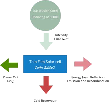
Figure 1 The thermodynamic of an isolated satellite
Shockley-Quessier Limit
It is critical to determine the upper limit of power production for a solar cell. The total amount of incoming radiation that can be converted as electrical power is defined as the efficiency of the solar cell. The upper limit of efficiency for any thin film solar is definitively bound by a set of balanced equations and was determined that no single cell could ever go beyond 33% in 1961.
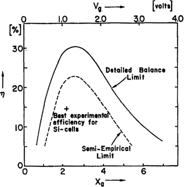
Figure 2 The “semiempirical limit” of efficiency of solar cells with the “detailed balance limit,” derived in the paper (6)
Thin Film Solar Cell (Cu(In,Ga)Se2)
Gerald Pearson, Calvin Fuller and Daryl Chapin, produced silicon waffered solar cells with 6% efficiency by the 1954, 22 years later and the first thin layered 𝐶𝑢(𝐼𝑛, 𝐺𝑎)𝑆𝑒,solar cell was created. This was to contest with 𝐺𝑎𝐴𝑠, it is deposited in a n/p-type configuration. Chen et al, in 1993 investigated 𝐶𝑑𝑍𝑛𝑆, conduction layer 𝑍𝑛𝑂 n-type stack this produced an efficiency of 13.7% with a (𝐼𝑛, 𝐺𝑎), layer p- type and produced the flow of oxide majority carrier collection [7], [8].
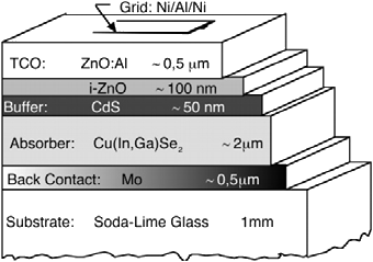
Figure 3 Structure a highly efficient thin film solar cell, with Cu(In,Ga)Se2 deposited absorbent layer, in this study different buffer layers are used[9]
The structure of the (𝐼𝑛, 𝐺𝑎), device comprises of Mo contact often on a Soda-lime glass substrate. Na diffusion from glass substrates have been shown through studies to increase optimal grain growth and carrier concentration, contributing to the 𝑉ij of the cell [10]–[12]. Depositing an even layer with grain formation is done by spluttering metal elements in a vacuum environment[13]. To match the p and n type energies and allow the separation of chargers, a buffer is applied. CdS requires chemical bath deposition (CBD) to form a uniformly, thin buffer layer on 𝐶𝑢(𝐼𝑛, 𝐺𝑎)𝑆𝑒. A thin n-type region of i− and 𝐴𝐼 − 𝑍𝑛𝑂 is deposited. 𝐴𝐼 − is doped AI to form a transparent conduction oxide layer that collects charges.
Buffer Layers
The purpose of a buffer layer in thin film solar cells is to form a coherent junction between layers, helping match the crystal lattice of different semi-conducting layers, so that multiple energy bands can be stack on top of each other[14]. Stacking layers of semi-conductor materials with dissimilar energy band form heterojunctions, for buffers it is optimal to have large energy gaps in contrast to the absorber, visible light will not be absorbed by the buffer, increasing the quantum efficiency[15]–[18].
Changing the concentration for the two crystalline structures that make up the absorbent layer 𝐶𝑢𝐼𝑛𝑆𝑒, and C𝑢𝐺𝑎𝑆𝑒,, modifies the concentration of crystalline phases and the energy band gap of the semi-conductor material. The (𝐼𝑛, 𝐺𝑎), tetragonal crystal is a complex structure and as such the deposited crystal will have imperfect junction interfaces. Surface recombination is an effect of unbonded (𝐼𝑛, 𝐺𝑎)𝑆𝑒, atoms between the junctions, it affects the efficiency of solar cell[19]. The unbonded atoms are considered defects of the junction, charged carriers can recombine to created defect states in the energy band gap. Lattice matching increases the open-circuit voltage 𝑉ij via reducing the number of defects. This shows a need for lattice matching of the buffer and the absorber. Similar lattice will reduce amount of surface defects. 𝐶𝑑𝑆 buffer layer exhibit diffusion of 𝐶𝑑 atoms this is reported to increase 𝑉ij [20].
Lattice matching is important to reduce surface recombination[21]. There are two ways of changing lattice structure changing both the composition of the absorber or changing the composition of the buffer. Crystal structure can often be hard to match as they can span over any three-dimensional axis. (𝐼𝑛, 𝐺𝑎)𝑆𝑒, have a tetrahedral structure, two coordinates are equal have equal distances, matching is made somewhat easier to do with this relation. The energy levels of the (𝐼𝑛, 𝐺𝑎), can be modified with by balancing ratios of 𝐺𝑎 to (𝐺𝑎 + 𝐼𝑛). This means allows for energy band gap tuning, in addition it changes the concentration of 𝐶𝑢𝐼𝑛𝑆𝑒_2 and 𝐶𝑢𝐺𝑎𝑆𝑒,.
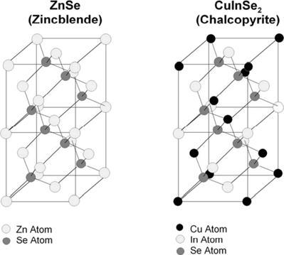
Figure 4 The tetragonal unit cell chalcopyrite phase for ZnSe and CuInSe2.[22]
The buffer/absorber energy bands are matched, such that the electrons and holes produce a current from the 𝐶𝑢(𝐼𝑛, 𝐺𝑎)𝑆𝑒, layer to the 𝑍𝑛𝑂 − 𝐴𝑖. The buffer and 𝐶𝑢(𝐼𝑛, 𝐺𝑎)𝑆𝑒, conduction band is a quantum step potential. A discrete step is made between the conduction bands between the buffer/absorber, aligning the high buffer step with the conduction band of 𝐶𝑢(𝐼𝑛, 𝐺𝑎)𝑆𝑒, allows tunneling to the 𝑍𝑛𝑂 −𝐴𝑖. The buffer layer must have low resistance for electron charge carriers to travel across the n-type layer. The tunneling current is a result of small thickness potential for the buffer and step of the energy levels. Buffers with aligned conduction bands will increase current flow to the electrode [16], [23].
Recombination Mechanisms
Electron energy states are given by the position of the fermi energy, there is an even distribution of electrons and holes in the conduction and valence states. Fermi levels is, heavily doped buffer have higher energy levels located to match the 𝐶𝑢(𝐼𝑛, 𝐺𝑎)𝑆𝑒,. The Fermi level splits in to consecutive charged carrier levels, the equation that govern the new Fermi levels are:


Electrons generated and the hole density state, determine the density in equilibrium of the corresponding electron density[24]. Fermi energy levels split allowing for additional states. In this case there is non-radiative recombination that occurs in the separate energy bands between the fermi levels, the splitting affect depends is created in defects and band bending.
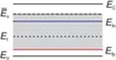
Figure 5 Band diagram of a p-type semiconductor.𝐸yyyqy denotes the demarcation level. If the energy level of a defect state 𝐸zis within the shaded area, the defect is an effective recombination center. Otherwise a captured electron is more likely to be re-emitted to the conduction band and the defect state is denoted as a trap.[25]
Current
For current in the solar cell to be increased to the maximum theoretical current, recombination loss mechanisms of charge carriers must be reduced. For (𝐼𝑛, 𝐺𝑎)𝑆𝑒, surface recombination, interface recombination’s and lattice mismatching that hinder the current in the solar cell. The recombination is spectrally affected, the low wavelength photons are strongly absorbed placing the generation of high energy photons at the front of the absorber. The buffer/absorber interface has defects and band bending that increases the rate combination for these high energy front charges. The measure of quantum efficiency is used measure the I-V curve of the 𝐶𝑢(𝐼𝑛, 𝐺𝑎)𝑆𝑒, solar cell.
Surface Recombination
Lattice mismatching significantly affects the performance of the (𝐼𝑛, 𝐺𝑎), solar cell. Any impurities or boundary defects at the junction of the solar cell increases surface recombination, this loss mechanism affects the electrical properties of the solar cell [26]. Since the junction of the (𝐼𝑛, 𝐺𝑎), cell has bonds of dissimilar semiconductor material there is severe disruption of lattice bonds, therefore the interfaces of the buffer/absorber and absorber/back contact are interfaces of particularly high surface recombination, like in the depletion layer of a semiconductor junction, where by majority carriers diffuse across the interface to equalize the imbalance of electrical fields, defects have an imbalance in charge concentrations that results in surrounding charges drift towards the surface[25]. Surface recombination is present in the (𝐼𝑛, 𝐺𝑎)𝑆𝑒,/Mo interface as extra dangling bonds extra energy states are created at the back, these defects are minimized through careful lattice matching, with the addition of the 𝐺𝑎 and 𝐶𝑢 to absorbent lay [27]. The buffer interface with the absorber share a heterojunction this means that the energy bands don’t align. Interface recombination is the major factor of recombination loss, where by the energy states makes charge recombination viable. Decreasing defects at these interfaces are important to reducing loss recombination.
Emissivity
One of the main reasons why solar cells lose performance is due to the temperature factor. Solar cells work at their best at low temperatures, but in space, they are commonly exposed to very high temperatures. According to the solar cell operating temperature equation, the higher the emissivity of a solar cell is, the higher operating temperature it will have. Moreover, the higher the emissivity is, the cooler the solar cell will be.
The most significant drawback of (𝐼𝑛, 𝐺𝑎), is its low emissivity (ε<0.2)[28] [29], which means that its surface is not very efficient in emitting the radiation it absorbed from the sun, back to the environment as thermal radiation. Thus, (𝐼𝑛, 𝐺𝑎), will not be able to cool down as desired and it will warm up even more than 100K [29], as it continues to expose to the sun emissions.
When radiation falls into a solar cell, it can be partially reflected (R=reflection), transmitted (T = transmission) or absorbed (A = absorption). According to the principle of conservation of energy, the relation between the three is as follows:

According to Kirchhoff’s law, at equilibrium for a given wavelength λ and temperature T, the emissivity of any body is equal to its absorption and for a uniform and a isotropic opaque surface in thermal equilibrium, the transmission is zero (for practical purpose, 𝐶𝑢(𝐼𝑛, 𝐺𝑎)𝑆𝑒, solar cells will be considered as a uniform and isotropic opaque Surface)[29]. In that case we have

and replacing this equation and T=0 on Equation 5, we will get:

It can be seen in Figure 6 that the low emissivity of 𝐶𝑢(𝐼𝑛, 𝐺𝑎)𝑆𝑒, solar cells is due to the high reflectance on the far-infrared zone (> 10𝜇𝑚) and because that spectral region represents more than 99% of the emissive power of a blackbody at room temperature[29]. To understand much more this value, it must be considered that emissivity represents the ratio of the emissive power of the body being investigated and the one for a black body at the same temperature as shown in spectral emissivity equation [29].

Because of all this and considering that emissivity in an integral as shown in Equation 9, low reflective coatings in the infrared spectral region must be developed to increase the emissivity and thus, the efficiency of the panel,

where 𝐸(𝜆)is the radiant heat of a grey body to its surroundings and 𝜎 = 5.67 × 10G§ 𝑊⁄𝑚, ∙ 𝐾ß the Stefan-Boltzmann constant.
Efficiency decreases very fast while temperature increases, and the objective here will be to describe that change with our own methods with the use of this equation

Where 𝐽/j is the short-circuit current density, 𝑉ij is already defined, FF is the fill factor and 𝑃öq is the total power of the incident light.
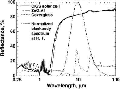
Figure 6 Reflectance as a function of wavelength.[30]Focusing on what is being analyzed, the 𝐶𝑢(𝐼𝑛, 𝐺𝑎)𝑆𝑒, curve it can be seen that the reflectance in the short-wavelength is very small compared to the long-wavelength
Temperature does not explicitly appear in this relationship, although 𝑉ij , 𝐽/j and FF are each functions of temperature. The equation below shows how 𝐽/j and 𝑉ij are related, so basically everything can be solve knowing the relation between both with temperature.

This equation shows how the open-circuit voltage relates with the short-circuit current density at a certain temperature and looking again at efficiency equation it will be more noticeable how closer we are to know how temperature really affects efficiency. The data of the voltage and current density used for the analysis are shown in the graphs below. 𝐽/j of 𝐶𝑢(𝐼𝑛, 𝐺𝑎)𝑆𝑒, relates with temperature almost in the same way than 𝑆𝑖 [28].
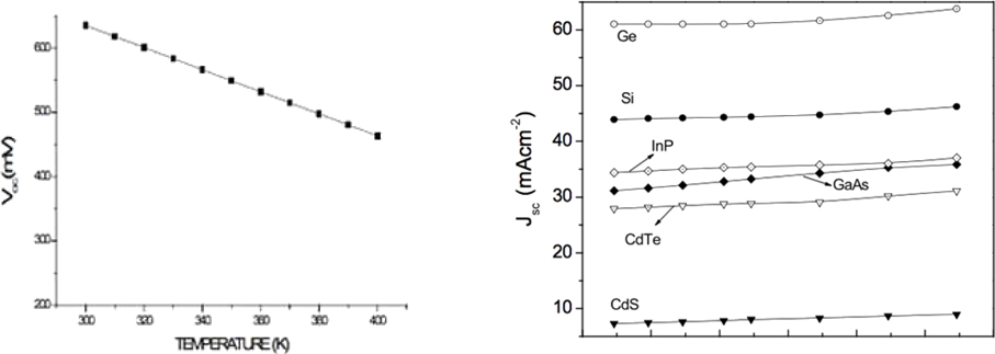
Figure 7 a) 𝑉ij as a function of temperature[29], b) 𝐽/j as a function of temperature [31]
Methods
(𝐼𝑛, 𝐺𝑎)𝑆𝑒, is a commonly studied thin film solar cell, it is one of the newer emerging second generation technology. Interest for the solar cell has been generated for its energy band control, direct and gap and to retain efficiency. Literature were referenced and analyzed through the search of the following array of data bases, UTS PAM, Mendeley, Scopus, UTS Library, ResearchGate.
Temperature Emissivity
For describing and analyzing how temperature affects the efficiency of (𝐼𝑛, 𝐺𝑎), solar cells and how increasing emissivity on the cell could help to offset the high temperatures that can be found in space- we analyzed every paper and found the basic parameters that control the efficiency of the panels for example 𝑉ij , 𝐽/j and Fill Factor. After that, we found the relation between emissivity values and operating temperature of two different types of coatings, 𝑆𝑖𝑂, single-layer and 𝑆𝑖𝑂,/𝐴𝑙,𝑂{ double-layer coatings and calculated the percentage of increase in emissivity that they contribute. For that, we used several equations, starting by the most important one, which shows how to calculate efficiency:

We started with the values of 𝑉ij at different temperatures that had been taken from another source and the value of 𝐽/j was set at 4.4 W/m2 as we concluded from various sources [11,12], an almost constant value for the range of temperatures we wanted to work with. After that, the fill factor was calculated according with the following formulas:

Where 𝑣ij is the normalized ij , 𝑞 = 1.6021726 × 𝐶 is the elementary charge, 𝑘 = 1.38064852 × 10G,{𝐶𝑉/𝐾) is the Boltzmann constant and 𝑇 is temperature in Kelvin. Now, it can also be set as a constant value, the power of the incident light, which at AM.0 conditions (conditions on which no atmosphere is above) is 13.5 W/m2. After that, it was easy to calculate the loss of efficiency while temperature increases using Equation 10.
Finally, the effect of emissivity over efficiency was investigated. For that, the following equation was used,

where 𝜀 is the emissivity, 𝛼 the absorptivity, 𝐼 = 𝑃öq and 𝜃 is the Stefan-Boltzmann constant (5.67𝑥10G§ 𝑊⁄𝑚, ∙ 𝐾ß). For practical purposes, the absorptivity was set as constant, although it depends in a certain way on emissivity, 𝜃 and 𝐼 were also set as constants, but this time because they truly are.
With that, we got an equation in which we could compare the two parameters we wanted to, it was found how each of the coatings affect the operating temperature.
For calculating the percentage of decrease in temperature of solar cells with different emissivities, operational temperature with an emissivity value of 0,18 will be used:

where 𝑇iw (𝜀) is the operational temperature of a solar cell with an emissivity value of 𝜀.
Buffer Layers
For finding the buffer layer that has the highest current in the 𝐶𝑢(𝐼𝑛, 𝐺𝑎)𝑆𝑒, solar cell we analyzed papers focusing on the buffer layers and found values for 𝑉ij , 𝐽/j and Fill Factor. The currently used buffer layer that were found 𝐶𝑑𝑆, (𝑂𝐻, 𝑆), , 𝑆𝑛𝑂,, 𝑍𝑛𝑂, 𝑍𝑛𝑆𝑛𝑂 and 𝑍𝑛𝑆. We collected papers that contained buffer layers and 𝐶𝑢(𝐼𝑛, 𝐺𝑎)𝑆𝑒, in the title. The parameters for each of the buffers are averaged and put into categorical table for each of the parameter. Sorting the graphs current and energy gap from highest to lowest a comparison was done.
Results and Discussion
Temperature Emissivity
As in can be seen in Graphic A in Figure 7a, 𝑉ij decreases a lot with temperature and in Figure 7b, although it cannot be appreciated very well, 𝐽/j increases with it, but at a lower rate. Figure 7b shows the effect of temperature on the 𝐽/j of several materials but (𝐼𝑛, 𝐺𝑎),. It is shown because although every material behaves differently, the rate in which its current-density changes is almost the same.
From Figure 7a, it is possible to estimate the fill factor of the (𝐼𝑛, 𝐺𝑎), at each temperature with Equation 12 taking some data from another source. Taking the value of 𝑉ij at each temperature and considering that at 300 K, 𝑉ij is equal to 0.65 and at 400 K is 0.45 and that the relation between 𝑉ij and temperature is linear, we get the following data:
The relation between temperature and the fill factor can also be seen in the graph below:
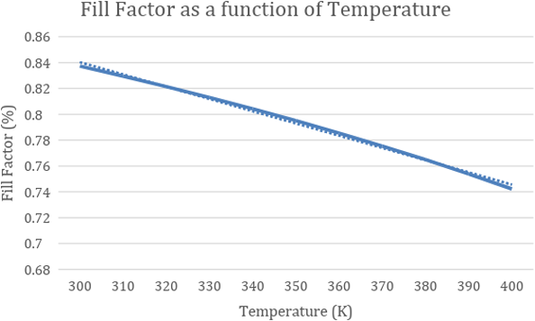
Figure 8 Fill Factor as a function of Temperature graph
Now, as in AM.0 conditions, solar intensity over solar 𝑃öq cells are 13 W/m2 [31][29], we now have all the data to calculate efficiency loss in solar cells as a product of temperature changes as shown in Equation 10. The results are shown below.
Plotting the results of Table 2, we will get the graph below (figure 9):
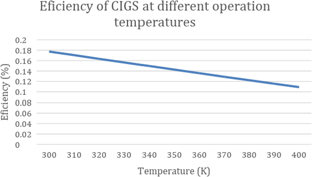
Figure 9 Effect of temperature over efficiency of (𝐼𝑛, 𝐺𝑎)
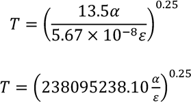
As it can be seen in Figure 9, the efficiency decreases at a rate of 0.07 percentage points per Kelvin. According to Equation 14, the operating temperature of (𝐼𝑛, 𝐺𝑎), depends on emissivity. Because the emissivity 𝜀 is part of the divisor of the formula, the bigger its value is, the lower the temperature of the solar cell will be. In that equation, it is already known the values of 𝜃, ; 5.67 × 10G§ 𝑊⁄𝑚, ∙ 𝐾ß and 13,50 𝑊/𝑚,, so now, Equation 13 will be:
For practical purposes 𝛼 is going to be taken as a constant, although we know it is not because it depends in some way on the value of 𝜀. We want to know which is going to be the effect of an increased emissivity value of the solar cell on its operating temperature, so this calculation is going to be only an approach of the real value.
The actual emissivity of a standardized 𝐶𝑢(𝐼𝑛, 𝐺𝑎)𝑆𝑒, solar cell is approximately 0,18 so in that case, the operating temperature of the cell at AM.0 conditions will be 190.71(𝛼)Z.,\𝐾. If emissivity is increased 0.1 to its actual value the resulting operating temperature will be 170.76(𝛼)Z.,\𝐾. If this last temperature is divided by the first one and then the resulting value is deducted from 1, the result will be the reduction percentage of the operating temperature, in this case 0.1. Nevertheless, we don´t have to forget that this is just an approach of the real value because 𝛼 is not being considered.
Different kind of coatings have been investigated in other papers for the same purpose, specially 𝑆𝑖𝑂, single layer and 𝑆𝑖𝑂,/𝐴𝑙,𝑂{ double layer coatings [31]. It has been shown by another research [30]that 2mm wide 𝑆𝑖𝑂, coating improves emissivity up to 0.65 and that 𝑆𝑖𝑂,/𝐴𝑙,𝑂{ coating of the same width increases it up to 0.78. With these values of emissivity, it is possible to us to calculate the percentage of decrease in operational temperature of solar cells with that coatings. 𝑆𝑖𝑂, coating will be able to reduce the operating temperature in a 27% and 𝑆𝑖𝑂,/𝐴𝑙,𝑂{ will do it on a 31%.
If we extrapolate values on the graphic of Figure 10 which shows efficiency as a function of operating temperature (𝜂 = −0.0007𝑇 + 0,3827) and if we suppose the standard temperature of the solar cell at AM.0 condition is 400K, the single layer coating could increase efficiency from 0.10886 to 0.17830 and the double layer coating from 0.10886 to 0.18950 or 63.4 % and 74.1 % respectively.
Buffer Layers
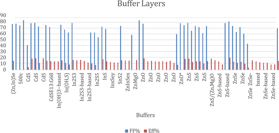
It was found that there is a direct relation of /j with the energy band gap of the buffers layer. These findings have are important for electrical performance. The spectral absorption of the buffer layers can overlap with the spectral absorption of the 𝐶𝑢(𝐼𝑛, 𝐺𝑎)𝑆𝑒,, this reduces the transmitted light to the absorb, denying blue light illumination. In Figure 14, the internal quantum efficiency is simulated for (𝑂, 𝑆) and 𝐶𝑑𝑆. It is seen that the internal quantum efficiency partial decreases around the wavelength that corresponds to 𝐶𝑑𝑆 energy band gap for the solar cell with 𝐶𝑑𝑆 as the buffer. It can be shown that the 𝐽/j is dependent on the energy gap of all the buffer analyzed, Figure 11 and Figure 12, shows that the ranking of 𝐽/j are identical to the energy, furthermore the magnitude of that separates them. This shows that the larger energy bands such as 𝑍𝑛𝑆 processes a higher quantum efficiency in the 𝐶𝑢(𝐼𝑛, 𝐺𝑎)𝑆𝑒, It has the largest energy bands. Further studies need to be done to determine whether the larger currents are more efficient cells and therefor 𝑍𝑛𝑆 should replace 𝐶𝑑𝑆 buffers in space applications.
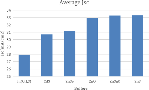
Figure 10 Averages of short circuit current the buffers
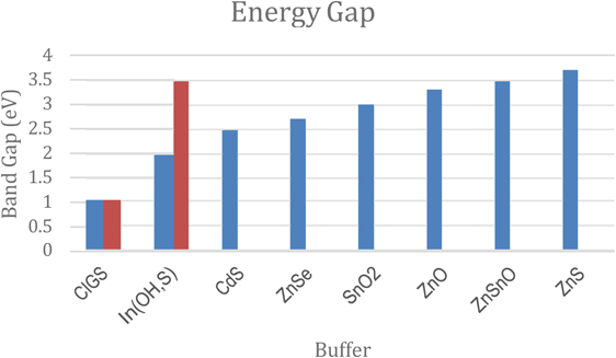
Figure 11 Energy gaps of the buffer layers from various literature, It is important to note that (𝑂𝐻, 𝑆) and (𝐼𝑛, 𝐺𝑎)𝑆𝑒, have energy levels that are dependent on there composition thus an upper and lower value is represented
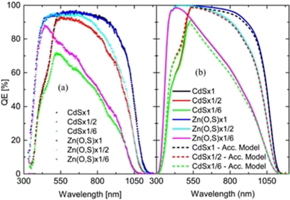
Figure 12 Measured and simulated internal quantum efficiency curves. Measurement are shown as scattered plots in (a) while solid and (b) dashed lines represent simulated data. Dashed lines show IQE-curves for the 𝐶𝑑𝑆 models with acceptor defects pinning the Fermi-level close to the (𝐼𝑛, 𝐺𝑎), valence band, at the buffer-absorber interface.[32]
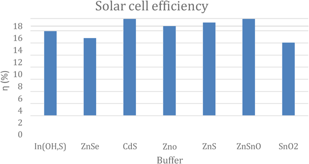
Figure 13 Averages of efficiency current the buffers
Conclusion
Space stations need highly efficient reliable solar cell to deal with the large energy consumption for human to habitat. The solar cell operating temperature on orbiting space station need to with stand high temperatures thermal cycles. High temperatures decreases efficiency of thin solar cells. Operating temperature of the solar cell is dependent on its optical emissivity; increasing emissivity was found to reduce the operational temperature of the cell and thus increase its overall efficiency. It was found that if the temperature of the solar cell is risen from 300K to 400K, its efficiency decreases in almost 8 percentage points, what means that at 400K the solar cell will be producing 39% less energy compared with its optimal conditions at 300 K. If that happens in the orbit about earth, in Venus, where the temperature above it is much higher compared with earth’s orbit, efficiency could decrease so much that the use of solar energy would no longer be optimal for that kind of missions. To offset all this, high-emissivity coating can be used over the solar cells to improve its emissivity. It was found that 𝑆𝑖𝑂, coating can decrease operating temperature a 27 % (i.e from 400K to 292K) and 𝑆𝑖𝑂,/𝐴𝑙,𝑂{ can decrease it on a 31% (i.e from 400K to 276K).
The buffer layer is found to heavily affect the electrical performance. Studying the effects buffer layers it was found that lattice matching, recombination loss of the charges, quantum efficiency and energy matching were all determined by the choice of buffer layer. Optical losses from certain buffer layer were, found from the Figure 13, of internal quantum efficiency. The low energy band gap from the 𝐶𝑑𝑆 buffer decreased the amount of quantum efficiency at high energy wavelengths, in the solar cell. Through the meta study a range of viable buffer layers were compared to determine the electrical effect that the energy band gaps had on the solar cells. It was found that current was dependent on the energy band gap. Buffer layers of ZnS are found to have the highest energy band producing the highest average current. This may be a viable replacement for 𝐶𝑑𝑆 as it will reduce the absorption of low wavelengths while producing high current. Further Studies on buffer layer should look at the effect of recombination’s and deposition techniques of high energy buffers to replace 𝐶𝑑𝑆 produce more efficient absorption for higher intensity space radiation.
Acknowledgments
We would like to thank Jurgen Schulte for his guidance. Thank you to Kieran and Keith Clarke for their guidance
References and Notes
1. E. Howell, “International Space Station: Facts, History & Tracking,” Space.Com, 2018. [Online]. Available: https://www.space.com/16748-international-space-station.html. [Accessed: 14-May-2018].
2. “International Space Station (ISS) power system | EDN.” [Online]. Available: http://www.edn.com/design/power-management/4427522/International-Space-Station--ISS--power- system. [Accessed: 14-May-2018].
3. T. Ghosh, “International Space Station Thermally Induced Solar Array Base Loads.”
4. “Stephen Hawking Never Reached Space, But He Sought to Lift All of Humanity.” [Online]. Available: https://www.space.com/39981-stephen-hawking-space-exploration-advocate.html. [Accessed: 14-May- 2018].
5. “The blackbody temperature of a planet,” Earth, pp. 3–4.
6. D. Felipe da Silva, itabr Ezio Castejon Garcia, M. Petry Rodrigues, A. Barros Costa, and – adabarcos, “Analysis of External Heat Loads for the Itasat Satellite in Two Attitude Control Configurations: Spin and 3-Axis Stabilizations,” vol. 21, 2010.
7. T. D. Lee and A. U. Ebong, “A review of thin film solar cell technologies and challenges,” Renew. Sustain. Energy Rev., vol. 70, pp. 1286–1297, 2017. https://doi.org/10.1016/j.rser.2016.12.028
8. T. Cdte, “Thin-Film CdTe Photovoltaic T d CulnSe2 fogies Prepared for the ISES Solar World Congress,” no. August, 1993.
9. J. Schöldström, “Thermal radiation from Co-evaporated Cu(In,Ga)Se2 End point detection and process control,” Digit. Compr. Summ. Uppsala Diss. from Fac. Sci. Technololgy 909, 2012.
10. M. Bodeg Ård, K. Granath, and L. Stolt, “Growth of Cu(In,Ga)Se2 thin films by coevaporation using alkaline precursors,” Thin Solid Films, vol. 361–362, pp. 9–16, Feb. 2000. https://doi.org/10.1016/s0040-6090(99)00828-7
11. M. A. Contreras et al., “On the Role of Na and Modifications to Cu(In,Ga)Se 2 Absorber Materials Using Thin-MF (M=Na, K, Cs) Precursor Layers,” 1997.
12. Rudmann, “Effects of sodium on growth and properties of Cu(In,Ga)Se₂ thin films and solar cells,” 2004.
13. U. M. Berner, “Formation of Cu(In,Ga)Se 2 from solution processed sodium containing metal precursors.”
14. A. Niemegeers, M. Burgelman, R. Herberholz, U. Rau, D. Hariskos, and H.-W. Schock, “Model for electronic transport in Cu(In,Ga)Se2 solar cells,” Prog. Photovoltaics Res. Appl., vol. 6, no. 6: pp. 407– 421, Nov. 1998. https://doi.org/10.1002/(sici)1099-159x(199811/12)6:6<407::aid-pip230>3.0.co;2-u
15. F.-L. Tang et al., “Lattice structures and electronic properties of CIGS/CdS interface: First-principles calculations,” Chinese Phys. B, vol. 23, no. 7: p. 077301, Jul. 2014. https://doi.org/10.1088/1674-1056/23/7/077301
16. I. The, “Chapter 1 Buffer Layer for Thin Film Heterojunction Solar Cells,” pp. 1–26.
17. A. L. Fahrenbruch and R. H. Bube, Fundamentals of solar cells : photovoltaic solar energy conversion. Academic Press, 1983.
18. P. M. P. Salomé et al., “CdS and Zn1−xSnxOybuffer layers for CIGS solar cells,” Sol. Energy Mater. Sol. Cells, vol. 159, pp. 272–281, Jan. 2017.
19. W. A. Goddard, “Predicted roles of defects on band offsets and energetics at CIGS (Cu(In,Ga)Se 2 /CdS) solar cell interfaces and implications for improving performance,” J. Chem. Phys., vol. 141, no. 9: p. 094701, 2014. https://doi.org/10.1063/1.4893985
20. N. Naghavi et al., “Buffer layers and transparent conducting oxides for chalcopyrite Cu(In,Ga)(S,Se)2 based thin film photovoltaics: present status and current developments,” Prog. Photovoltaics Res. Appl., vol. 18, no. 6: pp. 411–433, Sep. 2010. https://doi.org/10.1002/pip.955
21. C. Sah, R. Noyce, and W. Shockley, “Carrier Generation and Recombination in P-N Junctions and P-N Junction Characteristics,” Proc. IRE, vol. 45, no. 9: pp. 1228–1243, Sep. 1957. https://doi.org/10.1109/jrproc.1957.278528
22. R. Klenk, “Characterisation and modelling of chalcopyrite solar cells,” Thin Solid Films, vol. 387, no. 1–2, pp. 135–140, May 2001. https://doi.org/10.1016/s0040-6090(00)01736-3
23. J. STERNER, “ALD Buffer Layer Growth and Interface Formation on Cu(In,Ga)Se2 Solar Cell Absorbers,” p. 51, 2004.
24. W. Shockley and W. T. Read, “Statistics of the Recombinations of Holes and Electrons,” Phys. Rev., vol. 87, no. 5: pp. 835–842, Sep. 1952. https://doi.org/10.1103/physrev.87.835
25. S. D. E. S. Hzb and E. Charge, “Charge carrier transport in Cu ( In , Ga ) Se 2 thin-film solar-cells studied by electron beam induced current and temperature and illumination dependent current voltage analyses Melanie Nichterwitz,” 2012.
26. A. L. Fahrenbruch and R. H. Bube, Fundamentals of solar cells : photovoltaic solar energy conversion. Academic Press, 1983.
27. N. Touafek and R. Mahamdi, “Back Surface Recombination Effect on the Ultra-Thin CIGS Solar Cells by SCAPS,” Int. J. Renew. Energy Res., vol. 4, no. 4: p. 958, 2014.
28. A. Ferouani, M. Merad Boudia, A. Cheknane, and B. Benyoucef, “Temperature Effect of Electrical Properties of Cigs Solar Cell,” J. Fundam. Appl. Sci., vol. 3, no. 1: p. 77, Sep. 2015. http://dx.doi.org/10.4314/jfas.v3i1.8
29. M. Günthner, M. Pscherer, C. Kaufmann, and G. Motz, “High emissivity coatings based on polysilazanes
30. for flexible Cu(In,Ga)Se2thin-film solar cells,” Sol. Energy Mater. Sol. Cells, vol. 123, pp. 97–103, Apr. 2014. https://doi.org/10.1016/j.solmat.2014.01.027
31. X. He, Y. Li, L. Wang, and Y. Sun, “High emissivity coatings for high temperature application: Progress and prospect,” Thin Solid Films, vol. 517, no. 17: pp. 5120–5129, Jul. 2009. https://doi.org/10.1016/j.tsf.2009.03.175
32. P. Singh and N. M. Ravindra, “Temperature dependence of solar cell performance - An analysis,” Sol. Energy Mater. Sol. Cells, vol. 101, pp. 36–45, 2012. https://doi.org/10.1016/j.solmat.2012.02.019
33. J. Pettersson, T. Torndahl, C. Platzer-Bjorkman, A. Hultqvist, and M. Edoff, “The Influence of Absorber Thickness on Cu(In,Ga)Se Solar Cells With Different Buffer Layers,” IEEE Journal of Photovoltaics, 2013. [Online]. Available: http://ieeexplore.ieee.org.nthulib- oc.nthu.edu.tw/ielx7/5503869/6596156/06579660.pdf?tp=&arnumber=6579660&isnumber=6596156%5C nhttp://ieeexplore.ieee.org.nthulib-oc.nthu.edu.tw/xpls/abs_all.jsp?arnumber=6579660&tag=1. [Accessed: 21-May-2018].
34. P. Chelvanathan, M. I. Hossain, and N. Amin, “Performance analysis of copper-indium-gallium-diselenide (CIGS) solar cells with various buffer layers by SCAPS,” Curr. Appl. Phys., vol. 10, no. SUPPL. 3, pp. S387–S391, May 2010. https://doi.org/10.1016/j.cap.2010.02.018
35. P. Xin, J. K. Larsen, F. Deng, and W. N. Shafarman, “Development of Cu(In,Ga)Se2 superstrate devices with alternative buffer layers,” Sol. Energy Mater. Sol. Cells, vol. 157, pp. 85–92, Dec. 2016. https://doi.org/10.1016/j.solmat.2016.05.018
36. M. Moradi, R. Teimouri, M. Saadat, and M. Zahedifar, “Buffer layer replacement: A method for increasing the conversion efficiency of CIGS thin film solar cells,” Opt. - Int. J. Light Electron Opt., vol. 136, pp. 222–227, May 2017. https://doi.org/10.1016/j.ijleo.2017.02.037
37. S. Siebentritt, “Alternative buffers for chalcopyrite solar cells,” Sol. Energy, vol. 77, no. 6: pp. 767–775, Dec. 2004. https://doi.org/10.1016/j.solener.2004.06.018
38. D. Hariskos, S. Spiering, and M. Powalla, “Buffer layers in Cu(In,Ga)Se2 solar cells and modules,” Thin Solid Films, vol. 480–481, pp. 99–109, Jun. 2005. https://doi.org/10.1016/j.tsf.2004.11.118
39. J. Lindahl, J. T. Wätjen, A. Hultqvist, T. Ericson, M. Edoff, and T. Törndahl, “The effect of Zn 1− x Sn x O y buffer layer thickness in 18.0% efficient Cd-free Cu(In,Ga)Se 2 solar cells,” Prog. Photovoltaics Res. Appl., vol. 21, no. 8: pp. 1588–1597, Dec. 2013. https://doi.org/10.1002/pip.2239
Appendices
| Reference | Sample | FF (%) | η (%) | 𝑱𝒔𝒄 (mA/cm2) | 𝑽𝒐𝒄 (V) |
|---|---|---|---|---|---|
| [18] | CdS | 71.1 | 14.5 | 30.62 | 0.671 |
| [33] | CdS | 82.48575 | 21.533 | 33.654 | 0.777 |
| [33] | CdS | 74.4 | 15.1 | 30.5 | 0.666 |
| [34] | CdS | 41.3 | 4.3 | 25.5 | 0.406 |
| [35] | CdS | 77.49 | 18.72 | 35.14 | 0.687 |
| [35] | CdS | 78 | 19.2 | 35.7 | 0.689 |
| [36] | CdS | 72 | 11.4 | 21.8 | 0.729 |
| [37] | CdS | 19.2 | |||
| [38] | CdS | 76.5 | 17.9 | 32.9 | 0.714 |
| [36] | In(OH)3−based | 14 | |||
| [36] | In(OH)3−based | 14 | |||
| [36] | In(OH,S) | 75 | 15.7 | 35.5 | 0.594 |
| [36] | In(OH,S) | 67 | 11.4 | 23.2 | 0.735 |
| [36] | In(OH,S) | 62 | 9.1 | 10.7 | 0.685 |
| [36] | In2S3 | 78 | 16.4 | 31.5 | 0.665 |
| [36] | In2S3-based | 15.7 | |||
| [36] | In2S3-based | 16.4 | |||
| [37] | In2S3-based | 14.8 | |||
| [37] | In2S3-based | 12.2 | |||
| [36] | In2S5 | 62 | 8.2 | 20 | 0.661 |
| [33] | InS | 54.057 | 13.378 | 31.94 | 0.781 |
| [35] | InS | 71.74 | 17.61 | 35.45 | 0.692 |
| [36] | InS~5nm, iZnO 0.3% | 14.1 | 33.6 | 0.6614 | |
| [36] | InxSey | 13 | |||
| [36] | SnO2 | 12.2 | |||
| [36] | SnS2 | 12.2 | |||
| [36] | Zn(O,S) | 73 | 16 | 32 | 0.684 |
| [33] | ZnO | 82.4 | 21.178 | 33.144 | 0.776 |
| [35] | ZnO | 76.68 | 19.06 | 36.23 | 0.688 |
| [37] | ZnO | 14.3 | |||
| [37] | ZnO | 15 | |||
| [37] | ZnO | 14.2 | |||
| [37] | ZnO | 13.9 | |||
| [37] | ZnO | 14.6 | |||
| [37] | ZnO | 13.4 | |||
| [37] | ZnO | 15 | |||
| [37] | ZnO | 11.4 | |||
| [34] | ZnO* | 59.3 | 8.6 | 29.5 | 0.493 |
| [33] | ZnS | 77.5715 | 19.867 | 32.894 | 0.78 |
| [35] | ZnS | 74.11 | 18.32 | 35.73 | 0.691 |
| [36] | ZnS | 78 | 18.6 | 36.1 | 0.661 |
| [36] | ZnS | 73 | 14.4 | 34.2 | 0.578 |
| [36] | ZnS | 71 | 14.2 | 35.9 | ZnS |
| [36] | ZnS | 61 | 10.7 | 25.7 | 0.679 |
| [38] | ZnS/(Zn,Mg)O | 72.6 | 14.6 | 31.9 | 0.631 |
| [37] | ZnS-based | 14.2 | |||
| [37] | ZnS-based | 76.5 | 9.1 | ||
| [33] | ZnSe | 77.82875 | 20.622 | 33.856 | 0.782 |
| [35] | ZnSe | 80.49 | 20.07 | 36.15 | 0.689 |
| [36] | ZnSe | 73 | 13.6 | 34.4 | 0.554 |
| [36] | ZnSe | 71 | 13.4 | 34.3 | 0.551 |
| [36] | ZnSe | 60 | 10.1 | 23.7 | 0.713 |
| [34] | ZnSe* | 43.5 | 3.8 | 19.5 | 0.446 |
| [37] | ZnSe-based | 15.7 | |||
| [37] | ZnSe-based | 14.4 | |||
| [37] | ZnSe-based | 12.6 | |||
| [37] | ZnSe-based | 11.6 | |||
| [37] | ZnSe-based | 11.6 | |||
| [37] | ZnSe-based | 9.1 | |||
| [37] | ZnSe-based | 9 | |||
| [38] | ZnSnO | 73.9 | 17.6 | 34.8 | 0.682 |
| [18] | ZnSnO | 69.3 | 14.7 | 31.73 | 0.666 |